A Circuit and Systems Perspective notes
All figures and some content are taken and quoted, respectively, from the “A Circuit and Systems Perspective” textbook
Delay definitions
- Propagation delay time, = maximum time from the input crossing 50% to the output crossing 50%
- Contamination delay time, = minimum time from the input crossing 50% to the output crossing 50%
- Rise time, = time for a waveform to rise from 20% to 80% of its steady-state value
- Fall time, = time for a waveform to fall from 80% to 20% of its steady-state value
- Edge rate,
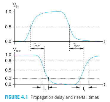
When an input changes, the output will retain its old value for at least the contamination delay and take the new value in at most the propagation delay.
Propagation delay and contamination delay times are also called max-time and min-time, respectively.
Propagation delay is usually the most relevant value of interest, and is often simply called delay.
Sequential and combination circuit
Combinational circuit: Output is a function of the current input
Sequential circuit: Output depends on previous as well as current inputs; such circuits are said to have state.
Sequential circuits are usually designed with flip-flops or latches, which are sometimes called memory elements, that hold data called tokens.
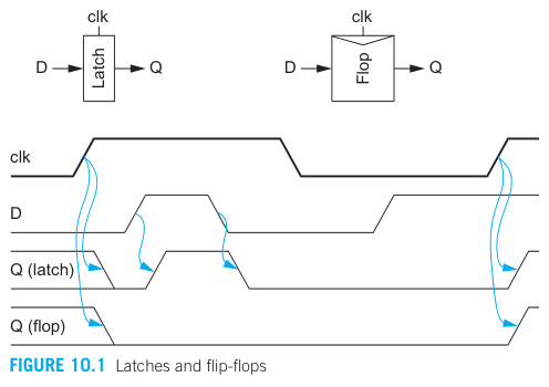
Sequencing static circuits
Latches and flip-flops are the most commonly used sequencing elements.
Sequencing methods
The below figures illustrating 3 methods of sequencing blocks of combinational logic. is clock period. In a 2-phase system, the phases maybe separated by the . In pulsed system, the pulse width is
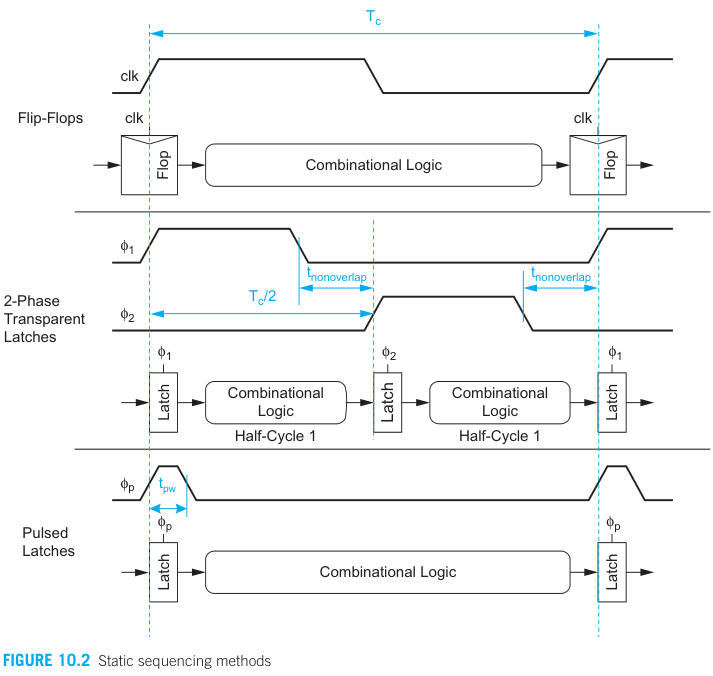
Flip-flop-based systems use one flip-flop on each cycle boundary. Tokens advance from one cycle to the next on the rising edge. If a token arrives too early, it waits at the flip-flop until the next cycle.
When the flip-flop is viewed as back-to-back pair of latches, if we separate the latches, the full cycle of combinational logic can be divided into 2 phases (half-cycle). 2 latch clocks are called and . The clocks can also be corresponded to nonoverlapping time ( > 0).
At least one clock is low and the coressponding latch is opaque → Preventing one token from catching up with other.
Pulsed latch systems eliminate one of the latches from each cycle and apply a brief pulse to the remaining latch. If the pulse is shorter than the delay through the combinational logic, we can still expect that a token will only advance through one clock cycle on each pulse.
Delays and timing constraints of the combinational logic and the sequencing elements
| Term | Name |
|---|---|
| Logic Propagation delay | |
| Logic Contamination delay | |
| Latch/Flop Clock-to-Q Propagation delay | |
| Latch/Flop Clock-to-Q Contamination delay | |
| Latch D-to-Q Propagation delay | |
| Latch D-to-Q Contamination delay | |
| Latch/Flop Setup time | |
| Latch/Flop Hold time |
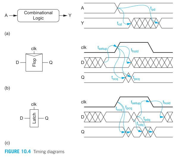
- (a):
- The output Y doesn’t change instantaneously.
- After the contamination delay , Y may begin to change or glitched
- After the propagation delay , Y must have settled to the final value.
- (b):
- The input D must have settled by some setup time before the rising edge of clk and should not change until a hold time *after the clock edge.
- The output Q begins to change after a clock-to-Q contamination delay and completely settles to the valid D value after a clock-to-Q propagation delay .
- (c):
- The input D must setup and hold around the falling edge that defines the end of the sampling period.
- The output initially started to change after , when the latch becomes transparent on the rising edge of the clock, and settles to input value after .
- If the input changed during the transparent state of the latch (i.e., clk is still asserted), the output will continue to track and reflect the input value after some D-to-Q delay and .
Negative hold time: The input can change before the clock edge and nevertheless the old level will be correctly recognized. → This can be produced by internal delay of the clock signal
Max-delay constraints
Assuming ideal clocks with no skew:
Flip-flop
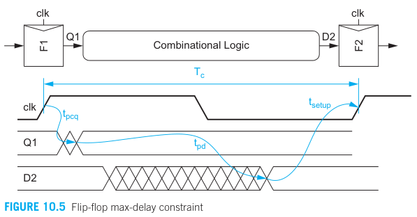
With this, the maximum allowable combinational logic delay:
Since F1 and F2 flip-flop is the same (assuming), the and for both F1 and F2 is the same
2-phase latch
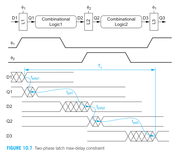
With this, the maximum allowable combinational logic delay
Pulsed latch
Only one latch is in the critical path in the pulsed latches cases. If the pulse is narrower than the setup time, the data must be setup before the pulse rises.
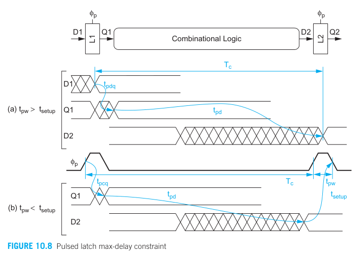
Solving the maximum combinational logic delay:
Min-delay constraints
Ideally, sequencing elements can be placed back-to-back without intervening the combinational logic and still function correctly.
If the hold time is large and the contamination delay is small → data can incorrectly propagate through 2 successive elements in one clock edge → corrupting the state of the system.
⇒ This is called race condition, hold-time failure, or min-delay failure.
Assuming the ideal clock is not skew:
Flip-flop
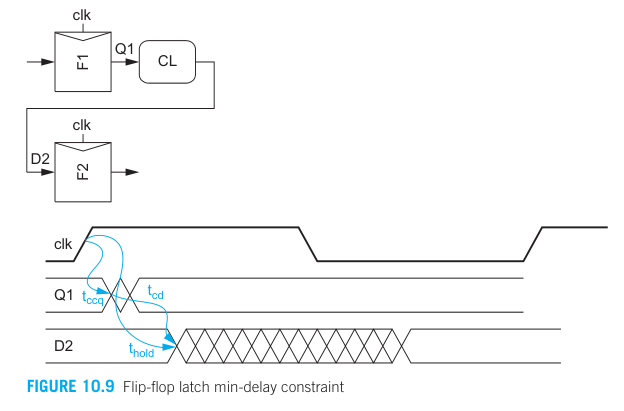
The data can begin to change at Q1 after a clk-to-Q contamination delay, and at D2 after another contamination logic delay. However, the changes must not reach D2 at least after the rise of clock edge (since the previous data is transmitting on D2, haven’t yet sampled at F2)
Hence, we solve the minimum logic contamination delay
If the contamination delay through the flip-flop exceeds the hold time, back-to-back flip-flops can safely be used. If not:
- Delay must be explicitly added between the flip-flops (e.g., with a buffer)
- Specical slow flip-flops with contamination delay greater than the contamination delay on the paths that require back-to-back flops.
2-phase latches
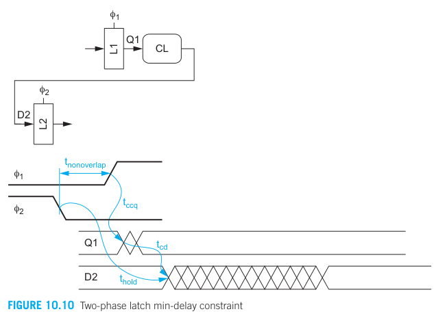
The data begins to pass through L1 on the rising edge of . It must not reach L2 until a hold time after the previous failing edge of because L2 must become safely opaque (deassert) before L1 becomes transparent.
Since the clock edges are separated by , the minimum logic contamination delay through each phase of logic is
⇒ By making the sufficiently large, hold-time failure can be avoided entirely.
However, generating and distributing nonoverlapping clocks is challenging at high speeds. Therefore, most commercial transparent latch-based systems use the clock and its complement. In this case, = 0 and the contamination delay constraint is the same as the constraint for the flip-flop.
The contamination delay constraint applies to each phase of the logic for latch-based system, but to the entire cycle of logic for flip-flops.
→ Seems like the latches required twice the overall logic contamination delay as compared to flip-flops (a paradox).
⇒ Since the flip-flop can be seen and built as a pair of latches, the mentioned paradox is resolved by observing that a flip-flop has an internal race condition between the 2 latches.
Pulsed latch
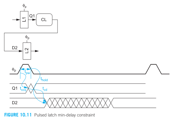
Data changes on the rising edge of the pulse but must hold until after the falling edge of the pulse → Pulse width effectively increases the hold time of the pulsed latch as compared to a flip-flop
Time borrowing
In system using flip-flops, data departs the first flop on the rising edge of the clock and must be set up at the second flop before the next rising edge of the clock.
- Data arrives late: Circuit provides wrong result
- Data arrives early: It is blocked until the clock edge, and the remaining time goes unused.
→ The clock imposes a hard edge because it sharply describe the cycles
In system using transparent latches, the data can depart from the first latch on the rising edge of the clock, but does not have to set up until the falling edge of the clock on the receiving latch.
If one half-cycle or stage of a pipeline has too much logic, it can borrow time into the next half-cycle or stage. Time borrowing can accumulate across multiple cycles.
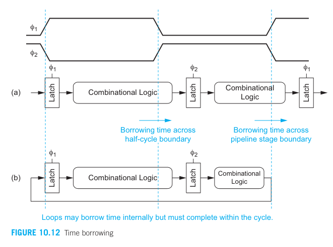
In system with feedback, the long delays must be balanced by shorter delays so that the overall loop completes in the time available.
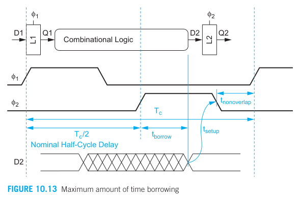
One phase can borrow up to half a cycle of time from the next (less setup time and non-overlap) since data does not have to set up until the falling edge of the receiving latch’s clock.
Clock skew
In reality, clocks have some uncertainty in their arrival times that can cut into the time available for useful computation.
The bold line: indicate the latest possible clock arrival time
The hashed line: show the clock might arrive over a range of earlier times because of the skew.
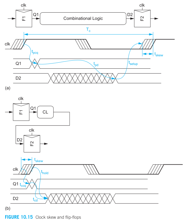
The worst case scenario for max delay in a flip-flop-based system is that the launching flop receives its clock late and the receiving flop recieves its clock early (Figure 10.15 (a))
→ The clock skew is subtracted from the time available for useful compuation and appears as sequencing overhead.
The worst case scenario for min delay is the launching flop receives its clock early and the receiving flop receives its clock late
→ The clock skew effectively increases the hold time of the system.
Resources
Weste, N., Harris, D., & Design, C. V. (2011). A Circuit and Systems Perspective. International Edition.